

-
2026 Chinese New Year Holiday
Dear Valued Customers/Partners, Please be informed that our company will be closed from February 11, 2026, to February 24, 2026, for the Chinese New Year (Spring Festival) holiday. Normal business operations will resume on February 25, 2026. During the holiday period, you may still send us inquir...Read more -

What Is the Purpose of the Multiple Capacitors on a Chip’s Power Supply Pins?
www.ankecircuit.com Mail: info@anke-pcb.com Whatapp/wechat:008618589033832 Skype: sannyduanbsp What Is the Purpose of the Multiple Capacitors on a Chip’s Power Supply Pins? As electronics engineers it is known that capacitors generally serve four primary functions: decou...Read more -
Time to prepare 2025 Chinese New Year Holiday
Dear Clients, With traditional Chinese New Year (CNY) comes, we are going to start holidays from 23rd Jan. to 5th Feb 2024, work will be renewed on 6th Feb 2025. Pls kindly consider this factor to avoid any inconvenience for your projects planning. Thanks a lot for attention and wish you succe...Read more -
National Day
Dear Clients, We are about to have the public holiday – National Day from 1th Oct to 7th Oct, work will be renewed on 8th Oct. Any mails during the time will be replied soon after back. Thanks for attention and wish you success! Shenzhen ANKE PCB Co.,LTD 2024-9-26Read more -

What are the considerations for PCB board colors
www.ankecircut.com www.anke-pcb.com Mail: info@anke-pcb.com Whatapp/wechat:008618589033832 Skype: sannyduanbsp What are the considerations for PCB board colors When it comes to the color of PCB boards, the most obvious thing to notice when receiving a PCB board is...Read more -
Laborl Day Holiday
Labor Day Dear Client, With Labor Day’s coming, we will have holidays from 1st May to 5th May, work will be renewed on 6th May. Any mails during the time will be replied soon after back. Thanks for attention and wish you all good! Shenzhen ANKE PCB Co.,LTD 2024-4-30Read more -
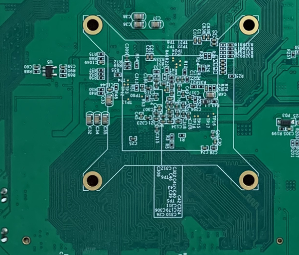
Three Aspects to secure power integrity in pcb designing
www.anke-pcb.com Mail: info@anke-pcb.com Whatapp/wechat:008618589033832 Skype: sannyduanbsp Three Aspects to secure power integrity in pcb designing In modern electronic design, power integrity is an indispensable part of PCB design. To ensure the stable operation and p...Read more -
Chinese New Year Holiday
Dear Clients, With traditional Chinese New Year (CNY) comes, we will have holidays from 5th Feb. to 17th Feb 2024, work will be renewed on 18th Feb 2024. Thanks a lot for attention and wish you succeed! Shenzhen ANKE PCB Co.,LTD 2024-1-31Read more -
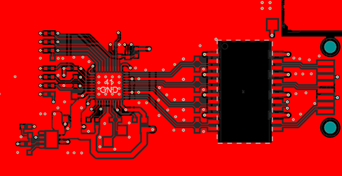
The essence of GND in circuits
www.ankecircuit.com Mail: info@anke-pcb.com Whatapp/wechat:008618589033832 Skype: sannyduanbsp The essence of GND in circuits During the PCB layouting process, engineers will face different GND treatments. Why does that happen? In the ...Read more -
Mid-Autumn Festival and National Day holiday
Dear Client, With Mid-Autumn Festival and National day’s approaching, we will have holidays from 29th Sept to 5th Oct, work will be renewed on 6th Oct. Thanks for attention and wish you all good! Shenzhen ANKE PCB Co.,LTD 2023-9-27Read more -
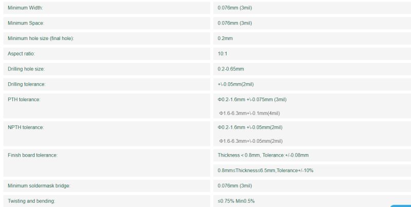
Line Width and Spacing rules in PCB designing
To achieve good PCB design, in addition to overall routing layout, the rules for line width and spacing are also crucial. That’s because line width and spacing determine the performance and stability of the circuit board. Therefore, this article will provide a detailed i...Read more -
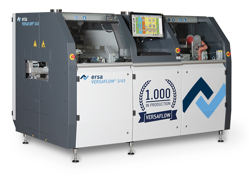
Selective soldering launching
In PCBA soldering process, the soldering of plug-in components on the PCBA usually involves manual soldering or traditional automated wave soldering, which entails avoiding surface-mounted SMT materials and certain non-tinned through-holes, requiring the customization of soldering fixtures. This ...Read more


