


Performing troubleshooting and repairs on PCBs can extend the lifespan of circuits. If a faulty PCB is encountered during the PCB assembly process, the PCB board can be repaired based on the nature of the malfunction. Below are some methods for troubleshooting and repairing PCBs.
1. How to perform quality control on PCB during the manufacturing process?
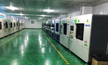
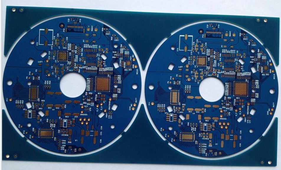
Typically, PCB factories have specialized equipment and essential processes that enable quality control of PCBs throughout the manufacturing process.
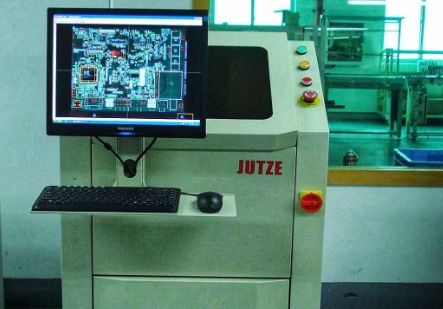
1.1. AOI Inspection
AOI inspection automatically scans for missing components, component misplacements, and other defects on the PCB. AOI equipment uses cameras to capture multiple images of the PCB and compares them with reference boards. When a mismatch is detected, it can indicate possible errors.
1.2. Flying Probe Testing
Flying probe testing is used to identify short and open circuits, incorrect components (diodes and transistors), and defects in diode protection. Various PCB repair methods can be used to correct shorts and component faults.
1.3. FCT Testing
FCT (Functional Test) primarily focuses on the functional testing of PCBs. The testing parameters are typically provided by engineers and may include simple switch tests. In some cases, specialized software and precise protocols may be required. Functional testing directly examines the functionality of the PCB under real-world environmental conditions.
2. Typical Causes of PCB Damage
Understanding the causes of PCB failures can help you quickly identify PCB faults. Here are some common errors:
Component failures: Replacing defective components can allow the circuit to function properly.
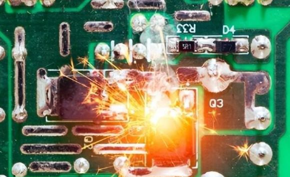
Overheating: Without proper heat management, some components may be burnt out.
Physical damage: This is mainly caused by rough handling,
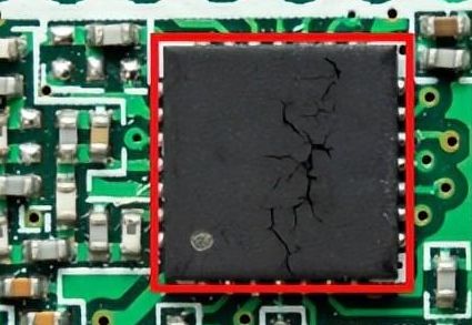
leading to cracks in components, solder joints, solder mask layers, traces, and pads.
Contamination: If the PCB is exposed to harsh conditions, traces and other copper components may be corroded.
3. How to Troubleshoot PCB Faults?
Following lists are 8 methods:
3-1. Understand the circuit schematic
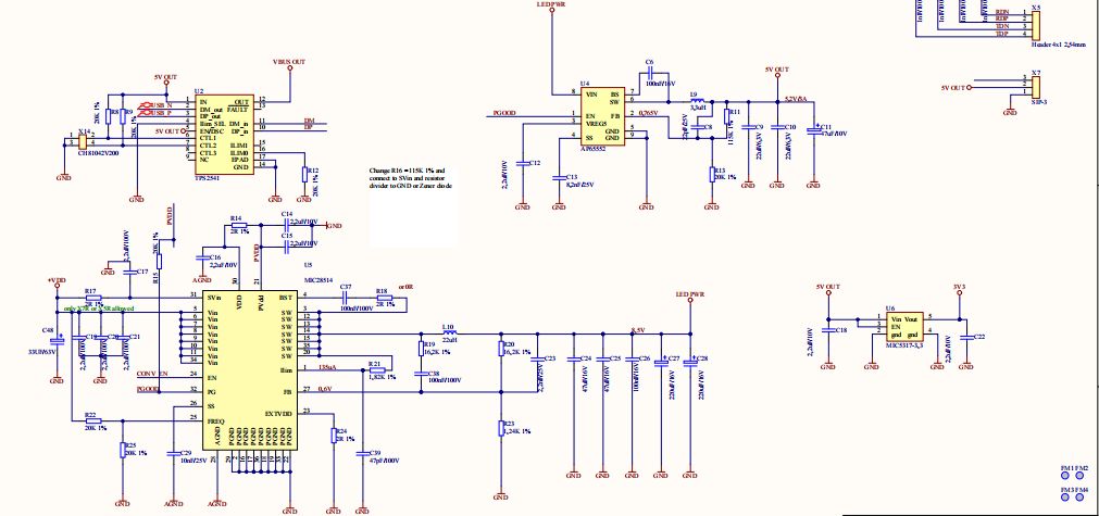
There are many components on the PCB, interconnected through copper traces. It includes power supply, ground, and various signals. Additionally, there are many circuits, such as filters, decoupling capacitors, and inductors. Understanding these is crucial for PCB repair.
Knowing how to trace the current path and isolate faulty sections relies on understanding the circuit schematic. If the schematic is unavailable, it may be necessary to reverse engineer the schematic based on the PCB layout.
3-2. Visual Inspection
As mentioned earlier, overheating is one of the main causes of PCB faults. Any burnt components, traces, or solder joints can easily be identified visually when there is no power input. Some examples of defects include:
- Bulging/overlapping/missing components
- Discolored traces
- Cold solder joints
- Excessive solder
- Tombstoned components
- Lifted/missing pads
- Cracks on the PCB
All of these can be observed through visual inspection.
3-3. Compare with an Identical PCB
If you have another identical PCB with one functioning properly and the other faulty, it becomes much easier. You can visually compare components, misalignments, and defects in traces or vias. Additionally, you can use a multimeter to check the input and output readings of both boards. Similar values should be obtained since the two PCBs are identical.
3-4. Isolate Faulty Components
When visual inspection is not sufficient, you can rely on tools such as a multimeter or an LCR meter. Test each component individually based on datasheets and design requirements. Examples include resistors, capacitors, inductors, diodes, transistors, and LEDs.
For instance, you can use the diode setting on a multimeter to check diodes and transistors. The base-collector and base-emitter junctions act as diodes. For simple circuit board designs, you can check for open and short circuits in all connections. Simply set the meter to resistance or continuity mode and proceed to test each connection.
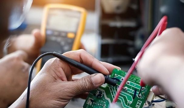
When conducting the checks, if the readings are within specifications, the component is considered to be functioning properly. If the readings are abnormal or higher than expected, there may be issues with the component or solder joints. Understanding the expected voltage at test points can aid in circuit analysis.
Another method for evaluating components is through nodal analysis. This method involves applying voltage to the selected components while not powering the entire circuit and measuring the voltage responses (V-response). Identify all the nodes and select the reference connected to important components or power sources. Use Kirchhoff's Current Law (KCL) to calculate the unknown node voltages (variables) and verify if these values match the expected ones. If there are issues observed at a particular node, it indicates a fault at that node.
3-5. Testing Integrated Circuits
Testing integrated circuits can be a substantial task due to their complexity. Here are some tests that can be performed:
- Identify all the markings and test the IC using a logic analyzer or an oscilloscope.
- Check if the IC is oriented correctly.
- Ensure that all solder joints connected to the IC are in good working condition.
- Evaluate the condition of any heat sinks or thermal pads connected to the IC to ensure proper heat dissipation.
3-6. Testing Power Supply
To troubleshoot power supply issues, it is necessary to measure rail voltages. The readings on a voltmeter can reflect the input and output values of components. Changes in voltage can indicate potential circuit problems. For instance, a reading of 0V on a rail may indicate a short circuit in the power supply, leading to component overheating. By conducting power integrity tests and comparing expected values to actual measurements, problematic power supplies can be isolated.
3-7. Identifying Circuit Hotspots
When visual defects cannot be found, physical inspection through power injection can be used to evaluate the circuit. Incorrect connections can generate heat, which can be felt by placing a hand on the circuit board. Another option is to use a thermal imaging camera, which is often preferred for low-voltage circuits. Necessary safety precautions should be taken to avoid electrical accidents.
One method is to ensure that you use only one hand for testing. If a hot spot is detected, it needs to be cooled down, and then all connection points should be checked to determine where the issue lies.
3-8. Troubleshooting with Signal Probing Techniques
To utilize this technique, it is crucial to have an understanding of the expected values and waveforms at test points. Voltage testing can be performed at various points using a multimeter, oscilloscope, or any waveform capture device. Analyzing the results can aid in isolating errors.
4. Tools Needed for PCB Repair
Before conducting any repairs, it is essential to gather the necessary tools for the job, as the saying goes, 'A blunt knife won't cut wood.'
● A worktable equipped with ESD grounding, power sockets, and lighting is essential.
● To limit thermal shocks, infrared heaters or preheaters may be required to preheat the circuit board.
● A precision drilling system is needed for slotting and hole opening during the repair process. This system allows control over the diameter and depth of the slots.
● A good soldering iron is necessary for soldering to ensure proper solder joints.
● In addition, electroplating may also be required.
● If the solder mask layer is damaged, it will need to be repaired. In such cases, an epoxy resin layer is preferable.
5. Safety Precautions during PCB Repair
It is important to take preventive measures to avoid safety accidents during the repair process.
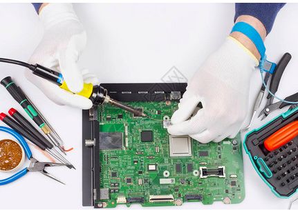
● Protective Equipment: When dealing with high temperatures or high power, wearing protective equipment is a must. Safety glasses and gloves should be worn during soldering and drilling processes, to protect against potential chemical hazards.
Wearing gloves while repairing PCBs.
● Electrostatic Discharge (ESD): To prevent electric shocks caused by ESD, make sure to unplug the power source and discharge any residual electricity. You can also wear grounding wristbands or use anti-static mats to further minimize the risk of ESD.
6. How to Repair a PCB?
Common faults in a PCB often involve defects in traces, components, and solder pads.
6-1. Repairing Damaged Traces
To repair broken or damaged traces on a PCB, use a sharp object to expose the surface area of the original trace and remove the solder mask. Clean the copper surface with a solvent to remove any debris, helping to achieve better electrical continuity.
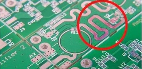
Alternatively, you can solder jumper wires to repair the traces. Ensure that the wire diameter matches the trace width for proper conductivity.
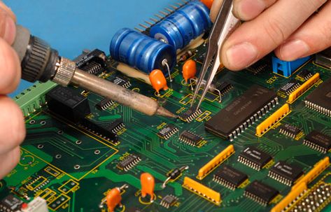
6-2. Replacing Faulty Components
Replacing damaged components
To remove faulty components or excessive solder from solder joints, it is necessary to melt the solder, but caution must be taken to avoid generating thermal stress on the surrounding surface area. Following the steps below to replace components in the circuit:
● Heat the solder joints quickly using a soldering iron or desoldering tool.
● Once the solder is melted, use a desoldering pump to remove the liquid.
● After removing all connections, the component will be detached.
● Next, assemble the new component and solder it in place.
● Trim the excess length of the component leads using wire cutters.
● Ensure that the terminals are connected according to the required polarity.
6-3. Repairing Damaged Solder Pads
With time moves on, solder pads on a PCB may lift, corrode, or break. Here are the methods for repairing damaged solder pads:
Lifted Solder Pads: Clean the area with a solvent using a cotton swab. To bond the pad back in place, apply conductive epoxy resin on the solder pad and press it down, allowing the epoxy resin to cure before continuing with the soldering process.
Damaged or Contaminated Solder Pads: Remove or cut away the damaged solder pad, exposing the connected trace by scraping off the solder mask around the pad. Clean the area with a solvent using a cotton swab. On the new solder pad (connected to the trace), apply a layer of conductive epoxy resin and secure it in place. Next, add epoxy resin between the trace and the solder pad. Cure it before proceeding with the soldering process.
Shenzhen ANKE PCB Co.,LTD
2023-7-20
Post time: Jul-21-2023


