


What is stack-up?
Stack-up refers to the arrangement of copper layers and insulating layers that make up a PCB prior to board layout design. While a layer stack-up allows you to get more circuitry on a single board through the various PCB board layers, the structure of PCB stackup design confers many other advantages:
• A PCB layer stack can help you minimize your circuit's vulnerability to external noise as well as minimize radiation and reduce impedance and crosstalk concerns on high-speed PCB layouts.
• A good layer PCB stack-up can also help you balance your needs for low-cost, efficient manufacturing methods with concerns about signal integrity issues
• The right PCB layer stack can enhance the Electromagnetic Compatibility of your design as well.
It will very often be to your benefit to pursue a stacked PCB configuration for your printed circuit board-based applications.
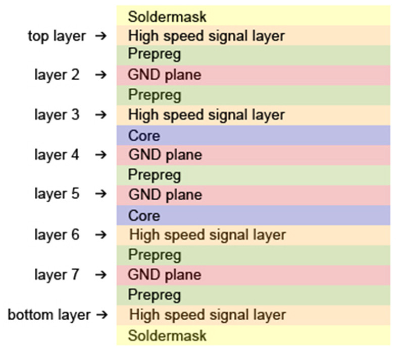
For multilayer PCBs, general layers include ground plane (GND plane), power plane (PWR plane), and inner signal layers. Here's a sample of an 8-layer PCB stackup.
ANKE PCB provides multilayer/high layers circuit boards in the range from 4 to 32 layers, board thickness from 0.2mm to 6.0mm, copper thickness from 18μm to 210μm (0.5oz to 6oz), inner layer copper thickness from 18μm to 70μm (0.5oz to 2oz), and minimal spacing between layers to 3mil.


