

Introduction
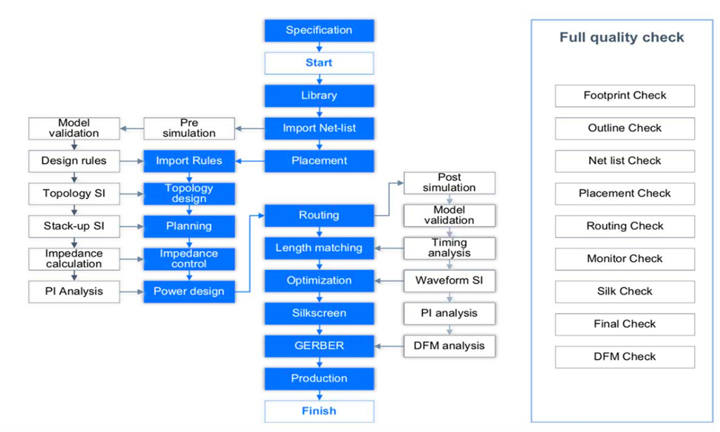
High Quality design
Well-built designing management system, strict inspection, effective deadline management makes the design no faulty-given
Senior designing team
10+ years of design experience design with manufacturing feasibility track and optimize from designing, simulation and production
Difficult design experience
High frequency, high speed and high density, digital and analog, large power and large current cases
Capability
Industry-leading designing,challenge the limits of the highest-end and most advanced manufacturing processes and design technologies.
46+
Layers
60000+
Pins
40000+
Connections
1521+
BGA pins
64+
BGA count 1 board
6mil+(3mil laser drill)
Vias
1+n+1/2+n+2/X+n+X
HDI build
360W-
Power consumption/pcb
4GHz+
Frequency
40Gbps+
Rate
0.44mm+
Pins spacing
3mil+
Width&spacing
Delivery Capacity
| Pin amount | Delivery (working days) |
| 0-2,000 | 3-5 |
| 2,000-4,000 | 5-8 |
| 4,000-6,000 | 8-12 |
| 6,000-8000 | 12-15 |
| 8,000-10,000 | 15-18 |
| 10,000-12,000 | 18-20 |
| 12,000-14,000 | 20-22 |
| 14,000-16,000 | 22-25 |


