


With the rapidly change of current modern life which requires much more additional processes that either optimize the performance of your circuit boards in relation to their intended use, or assist with multi-stage assembly processes to reduce labor and improve throughput efficiency, ANKE PCB is dedicating to upgrade new tech to meet client’s contieneously demands.
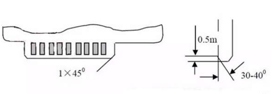
Edge connector bevelling for gold finger
Edge connector bevelling generally used in gold fingers for gold plated boards or ENIG boards, it is the cutting or shaping of an edge connector at an certain angle. Any beveled connectors PCI or other make it easier for the board to get into the connector. Edge Connector bevelling is a parameter in the order details that you need to select and check this option when required.
Carbon print
Carbon print are made of carbon ink and can be used for keyboard contacts, LCD contacts and jumpers. The printing is performed with conductive carbon ink.
Carbon elements must resist soldering or HAL.
Insulation or Carbon widths may not reduce below 75 % of the nominal value.
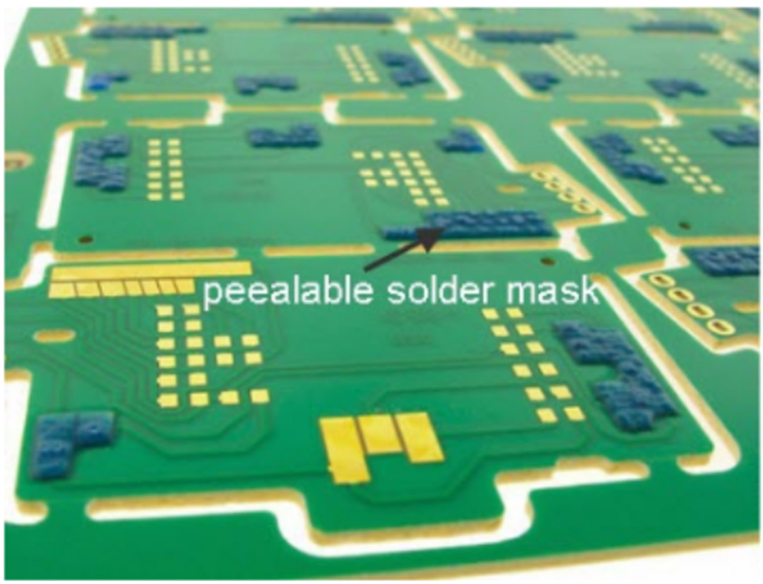
Sometimes a peelable mask is necessary to protect against used fluxes.
Peelable soldermask
Peelable soldermask The peelable resist layer is used to cover areas that are not to be soldered during the solder wave process. This flexible layer can then be subsequently removed easily to leave pads, holes and solderable areas perfect condition for secondary assembly processes and component/connector insertion.
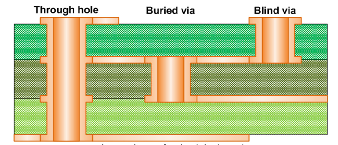
Blind & buried vais
What is Blind Via?
In a blind via, the via connects the external layer to one or more inner layers of the PCB and is responsible for the interconnection between that top layer and the inner layers.
What is Buried Via?
In a buried via, only the inner layers of the board are connected by the via. It is "buried" inside the board and not visible from the outside.
Blind and buried vias are especially beneficial in HDI boards because they optimize board density without increasing board size or the number of board layers required.
How to make blind&buried vias
Generally We don’t use depth-controlled laser drilling to manufacture blind and buried vias. Firstly we drill one or more cores and plate through the holes. Then we build and press the stack. This process can be repeated several times.
This means:
1. A Via always has to cut through an even number of copper layers.
2. A Via cannot end at the top side of a core
3. A Via cannot start at the bottom side of a core
4. Blind or Buried Vias cannot start or end inside or at the end of another Blind/Buried via unless the one is completely enclosed within the other (this will add extra cost as an extra press cycle is required).
Impedance control
Impedance control has been one of the essential concerns and severe problems in high-speed pcb design.
In high-frequency applications, controlled impedance helps us ensure that signals are not degraded as they route around a PCB.
Resistance and reactance of an electrical circuit have a significant impact on functionality, as specific processes must be completed before others to ensure proper operation.
Essentially, controlled impedance is the matching of substrate material properties with trace dimensions and locations to ensure the impedance of a trace's signal is within a certain percentage of a specific value.


