


Mail: info@anke-pcb.com
Whatapp/wechat:008618589033832
Skype: sannyduanbsp
Three Aspects to secure power integrity in pcb designing
In modern electronic design, power integrity is an indispensable part of PCB design. To ensure the stable operation and performance of electronic devices, we must consider and design comprehensively from the power source to the receiver.
Through carefully designing and optimizing power modules, inner layer planes, and power supply chips can we truly achieve power integrity. This article will delve into these three key aspects to provide practical guidance and strategies for PCB designers.
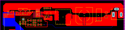
I. Power Module Layout Wiring
The power module is the energy source of every electronic devices, its performance and layout directly affect the stability and efficiency of the entire system. The correct layout and routing can not only reduce noise interference but also ensure smooth current flow, thereby improving overall performance.
2.Power module layout
1.Source processing:
The power module should be paid special attention since it serves as the starting point of the power. To reduce noise introduction, the environment around the power module should be kept as clean as possible to avoid adjacency to other high-frequency or noise-sensitive components.
2.Close to the power supply chip:
The power module should be placed as close to the power-supplied chip as possible. This can reduce losses in the current transmission process and reduce the area requirements of the inner layer plane.
3.Heat dissipation considerations:
The power module may generate heat during operation, so it should be ensured that there are no obstructions above it for heat dissipation. If necessary, heatsinks or fans can be added for cooling.
4.Avoiding loops:
When routing, avoid forming current loops to reduce the possibility of electromagnetic interference.
II. Inner Layer Plane Design Planning
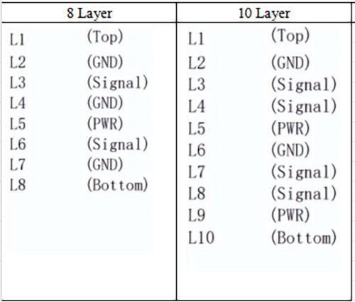
A. Layer stack design
In PCB EMC design, layer stack design is a key element that needs to consider routing and power distribution.
a. To ensure low impedance characteristics of the power plane and absorb ground noise coupling, the distance between power and ground planes should not exceed 10mil, typically recommended to be less than 5mil.
b. If a single power plane cannot be implemented, a surface layer can be used to lay out the power plane. The closely adjacent power and ground planes form a plane capacitor with minimum AC impedance and excellent high-frequency characteristics.
c. Avoid adjacent two power layers, especially with large voltage differences, to prevent noise coupling. If unavoidable, increase the spacing between the two power layers as much as possible.
d. Reference planes, especially power reference planes, should maintain low impedance characteristics and can be optimized through bypass capacitors and layer adjustments.
B.Multiple power segmentation
a. For specific small-range power sources, such as the core working voltage of a certain IC chip, copper should be laid on the signal layer to ensure the integrity of the power plane, but avoid laying power copper on the surface layer to reduce noise radiation.
b. The selection of segmentation width should be appropriate. When the voltage is greater than 12V, the width can be 20-30mil; otherwise, choose 12-20mil. The segmentation width between analog and digital power sources needs to be increased to prevent digital power from interfering with analog power.
c. Simple power networks should be completed on the routing layer, and longer power networks should have filter capacitors added.
d. The segmented power plane should be kept regular to avoid irregular shapes causing resonance and increased power impedance. Long and narrow strips and dumbbell-shaped divisions are not allowed.
c.Plane filtering
a. The power plane should be closely coupled with the ground plane.
b. For chips with operating frequencies exceeding 500MHz, primarily rely on plane capacitor filtering and use a combination of capacitor filtering. The filtering effect needs to be confirmed by power integrity simulation.
c. Install inductors for decoupling capacitors on the control plane, such as widening capacitor leads and increasing capacitor vias, to ensure that the power ground impedance is lower than the target impedance.
III. Power Chip Layout Wiring
The power chip is the core of electronic devices, and ensuring its power integrity is crucial for improving device performance and stability. Power integrity control for power chips mainly involves routing handling of chip power pins and correct layout and wiring of decoupling capacitors. The following will detail considerations and practical advice regarding these aspects.
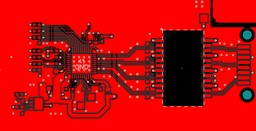
A.Chip power pin routing
The routing of chip power pins is a crucial part of power integrity control. To provide a stable current supply, it is recommended to thicken the routing of power pins, generally to the same width as the chip pins. Typically, the minimum width should not be less than 8mil, but for better results, try to achieve a width of 10mil. By increasing the routing width, impedance can be reduced, thus reducing power noise and ensuring sufficient current supply to the chip.
B.Layout and routing of decoupling capacitors
Decoupling capacitors play a significant role in power integrity control for power chips. Depending on capacitor characteristics and application requirements, decoupling capacitors are generally divided into large and small capacitors.
a. Large capacitors: Large capacitors are usually evenly distributed around the chip. Due to their lower resonant frequency and larger filtering radius, they can effectively filter out low-frequency noise and provide stable power supply.
b. Small capacitors: Small capacitors have a higher resonant frequency and smaller filtering radius, so they should be placed as close as possible to the chip pins. Placing them too far away may not effectively filter out high-frequency noise, losing the decoupling effect. Correct layout ensures that the effectiveness of small capacitors in filtering high-frequency noise is fully utilized.
C.Wiring method of parallel decoupling capacitors
To further improve power integrity, multiple decoupling capacitors are often connected in parallel. The main purpose of this practice is to reduce the equivalent series inductance (ESL) of individual capacitors through parallel connection.
When paralleling multiple decoupling capacitors, attention should be paid to the placement of vias for capacitors. A common practice is to offset the vias of the power and ground. The main purpose of this is to reduce the mutual inductance between decoupling capacitors. Ensure that the mutual inductance is much smaller than the ESL of a single capacitor, so that the overall ESL impedance after paralleling multiple decoupling capacitors is 1/N. By reducing mutual inductance, filtering efficiency can be effectively enhanced, ensuring improved power stability.
Layout and routing of power modules, inner layer plane design planning, and correct handling of power chip layout and wiring are indispensable in electronic device design. Through proper layout and routing, we can ensure the stability and efficiency of power modules, reduce noise interference, and improve overall performance. Layer stack design and multiple power segmentation further optimize the characteristics of power planes, reducing power noise interference. Proper handling of power chip layout and wiring and decoupling capacitors are crucial for power integrity control, ensuring a stable current supply and effective noise filtering, enhancing device performance and stability.
In practical working, various factors such as current magnitude, routing width, number of vias, coupling effects, etc., need to be comprehensively considered to make rational layout and routing decisions. Follow design specifications and best practices to ensure control and optimization of power integrity. Only in this way can we provide stable and efficient power supply for electronic devices, meet the increasing performance demands, and drive the development and progress of electronic technology.
Shenzhen ANKE PCB Co.,LTD
Post time: Mar-25-2024


