


To achieve good PCB design, in addition to overall routing layout, the rules for line width and spacing are also crucial. That’s because line width and spacing determine the performance and stability of the circuit board. Therefore, this article will provide a detailed introduction to the general design rules for PCB line width and spacing.
It is important to note that the software default settings should be properly configured and the Design Rule Check (DRC) option should be enabled before routing. It is recommended to use a 5mil grid for routing, and for equal lengths 1mil grid can be set based on the situation.
PCB Line Width Rules:
1.Routing should first meet the manufacturing capability of the factory. Confirm the production manufacturer with the customer and determine their production capability. If no specific requirements are provided by the customer, refer to impedance design templates for line width.
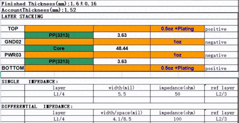
2.Impedance templates: Based on the provided board thickness and layer requirements from the customer, select the appropriate impedance model. Set the line width according to the calculated width inside the impedance model. Common impedance values include single-ended 50Ω, differential 90Ω, 100Ω, etc. Note whether the 50Ω antenna signal should consider reference to the adjacent layer. For common PCB layer stackups as reference below.
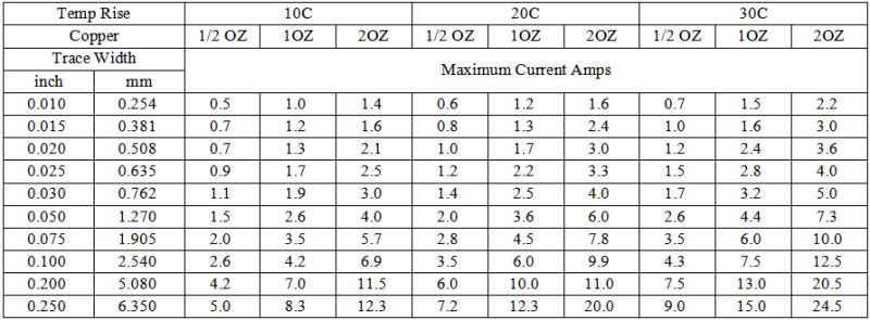
3.As shown in the diagram below, the line width should meet the current-carrying capacity requirements. In general, based on experience and considering routing margins, the power line width design can be determined by the following guidelines: For a temperature rise of 10°C, with 1oz copper thickness, a 20mil line width can handle an overload current of 1A; for 0.5oz copper thickness, a 40mil line width can handle an overload current of 1A.
4. For general design purposes, the line width should preferably be controlled above 4mil, which can meet the manufacturing capabilities of most PCB manufacturers. For designs where impedance control is not necessary (mostly 2-layer boards), designing a line width above 8mil can help to reduce the manufacturing cost of the PCB.
5. Consider the copper thickness setting for the corresponding layer in the routing. Take 2oz copper for instance,try to design the line width above 6mil. The thicker the copper, the wider the line width. Ask for the manufacturing requirements of the factory for non-standard copper thickness designs.
6. For BGA designs with 0.5mm and 0.65mm pitches, a 3.5mil line width can be used in certain areas (can be controlled by design rules).
7. HDI board designs can use a 3mil line width. For designs with line widths below 3mil, it is necessary to confirm the production capability of the factory with the customer, as some manufacturers can only capable of 2mil line widths (can be controlled by design rules). Thinner line widths increase manufacturing costs and extend the production cycle.
8. Analog signals (such as audio and video signals) should be designed with thicker lines, typically around 15mil. If space is limited, the line width should be controlled above 8mil.
9. RF signals should be handled with thicker lines, with reference to adjacent layers and impedance controlled at 50Ω. RF signals should be processed on the outer layers, avoiding internal layers and minimizing the use of vias or layer changes. RF signals should be surrounded by a ground plane, with the reference layer preferably being the GND copper.
PCB Wiring Line Spacing Rules
1. The wiring should first meet the processing capacity of the factory, and the line spacing should meet the production capability of the factory, generally controlled at 4 mil or above. For BGA designs with 0.5mm or 0.65mm spacing, a line spacing of 3.5 mil can be used in some areas. HDI designs can choose a line spacing of 3 mil. Designs below 3 mil must confirm the production capability of the manufacturing factory with the customer. Some manufacturers have a production capability of 2 mil (controlled in specific design areas).
2. Before designing the line spacing rule, consider the copper thickness requirement of the design. For 1 ounce copper try to maintain a distance of 4 mil or above, and for 2 ounce copper, try to maintain a distance of 6 mil or above.
3. The distance design for differential signal pairs should be set according to impedance requirements to ensure proper spacing.
4. The wiring should be kept away from the board frame and try to ensure that the board frame can have ground (GND) vias. Keep the distance between signals and board edges above 40 mil.
5. The power layer signal should have a distance of at least 10 mil from the GND layer. The distance between the power and power copper planes should be at least 10 mil. For some ICs (such as BGAs) with smaller spacing, the distance can be adjusted appropriately to a minimum of 6 mil (controlled in specific design areas).
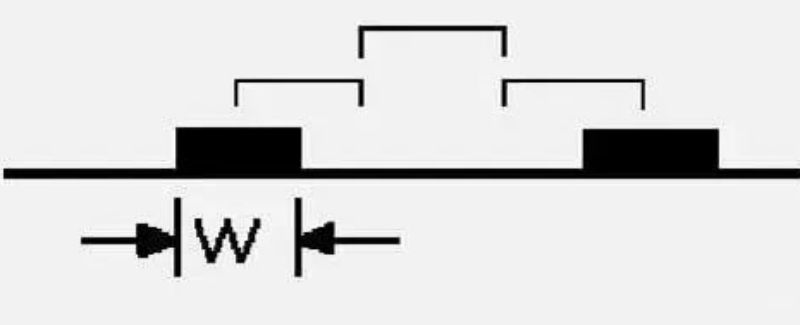
6.Important signals like clocks, differentials, and analog signals should have a distance of 3 times the width (3W) or be surrounded by ground (GND) planes. The distance between lines should be kept at 3 times the line width to reduce crosstalk. If the distance between the centers of two lines is not less than 3 times the line width, it can maintain 70% of the electric field between the lines without interference, which is known as the 3W principle.
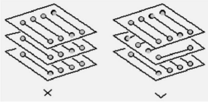
7.Adjacent layer signals should avoid parallel wiring. The routing direction should form an orthogonal structure to reduce unnecessary interlayer crosstalk.
8. When routing on the surface layer, keep a distance of at least 1mm from the mounting holes to prevent short circuits or line tearing due to installation stress. The area around screw holes should be kept clear.
9. When dividing power layers, avoid excessively fragmented divisions. In one power plane, try not to have more than 5 power signals, preferably within 3 power signals, to ensure current carrying capacity and avoid the risk of signal crossing the split plane of adjacent layers.
10.Power plane divisions should be kept as regular as possible, without long or dumbbell-shaped divisions, to avoid situations where the ends are large and the middle is small. The current carrying capacity should be calculated based on the narrowest width of the power copper plane.
Shenzhen ANKE PCB Co.,LTD
2023-9-16
Post time: Sep-19-2023


