


The holes on PCB can be classified into plated through holes (PTH) and non-plated through holes (NPTH) based on if they have electrical connections.
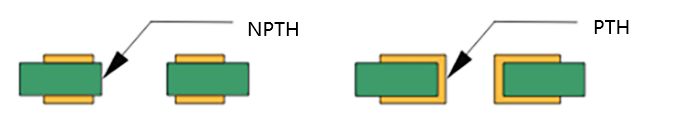
Plated through hole (PTH) refers to a hole with a metal coating on its walls, which can achieve electrical connections between conductive patterns on the inner layer, outer layer, or both of a PCB. Its size is determined by the size of the drilled hole and the thickness of the plated layer.
Non-plated through holes (NPTH) are the holes that do not participate in the electrical connection of a PCB, also known as non-metalized holes. According to the layer that a hole penetrates through on the PCB, holes can be classified as through-hole, buried via/hole, and blind via/hole.
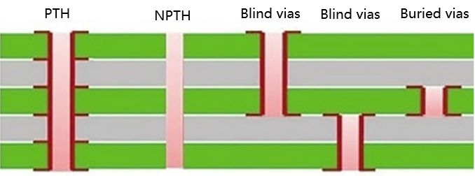
Through-holes penetrate the entire PCB and can be used for internal connections and/or positioning and mounting of components. Among them, the holes used for fixing and/or electrical connections with component terminals (including pins and wires) on the PCB are called component holes. Plated through-holes used for internal layers connections but without mounting component leads or other reinforcement materials are called via holes. There are mainly two purposes for drilling through-holes on a PCB: one is to create an opening through the board, allowing subsequent processes to form electrical connections between the top layer, bottom layer, and inner layer circuits of the board; the other is to maintain the structural integrity and positioning accuracy of component installation on the board.
Blind vias and buried vias are widely used in high-density interconnect (HDI) technology of HDI pcb, mostly in high layers pcb boards. Blind vias typically connect the first layer to the second layer. In some designs, blind vias can also connect the first layer to the third layer. By combining blind and buried vias, more connections and higher circuit board densities required of HDI can be achieved. This allows for increased layer densities in smaller devices while improving power transmission. Hidden vias help keep circuit boards lightweight and compact. Blind and buried via designs are commonly used in complex-design, light-weighting, and high-costing electronic product such as smartphones, tablets, and medical devices.
Blind vias are formed by controlling the depth of drilling or laser ablation. The latter is currently the more common method. The stacking of via holes is formed through sequential layering. The resulting via holes can be stacked or staggered, adding additional manufacturing and testing steps and increasing costs.
According to the purpose and function of the holes, they can be classified as:
Via holes:
They are metalized holes used to achieve electrical connections between different conductive layers on a PCB, but not for the purpose of mounting components.
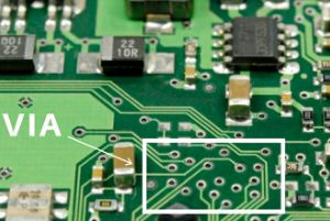
PS: Via holes can be further classified into through-hole, buried hole, and blind hole, depending on the layer that the hole penetrates through on the PCB as mentioned above.
Component holes:
They are used for soldering and fixing plug-in electronic components, as well as for through-holes used for electrical connections between different conductive layers. Component holes are typically metalized, and can also serve as access points for connectors.
Mounting holes:
They are larger holes on the PCB used for securing the PCB to a casing or other support structure.
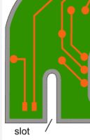
Slot holes:
They are formed either by automatically combining multiple single holes or by milling grooves in the drilling program of the machine. They are generally used as mounting points for connector pins, such as the oval-shaped pins of a socket.
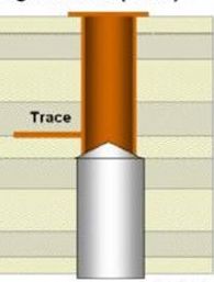
Backdrill holes:
They are slightly deeper holes drilled into plated-through holes on the PCB to isolate the stub and reduce signal reflection during transmission.
Followings are some auxiliary holes that PCB manufacturers may use in the PCB manufacturing process that PCB design engineers should be familiar with:
● Locating holes are three or four holes on the top and bottom of the PCB. Other holes on the board are aligned with these holes as a reference point for positioning pins and fixing. Also known as target holes or target position holes, they are produced with a target hole machine (optical punching machine or X-RAY drilling machine, etc.) before drilling, and used for positioning and fixing pins.
● Inner layer alignment holes are some holes on the edge of the multilayer board, used to detect if there is any deviation in the multilayer board before drilling within the graphic of the board. This determines whether the drilling program needs to be adjusted.
● Code holes are a row of small holes on one side of the bottom of the board used to indicate some production information, such as product model, processing machine, operator code, etc. Nowadays, many factories use laser marking instead.
● Fiducial holes are some holes of different sizes on the edge of the board, used to identify if the drill diameter is correct during the drilling process. Nowadays, many factories use other technologies for this purpose.
● Breakaway tabs are plating holes used for PCB slicing and analysis to reflect the quality of the holes.
● Impedance test holes are plated holes used for testing the impedance of the PCB.
● Anticipation Holes are normally non-plated holes used to prevent the board being positioned backwards, and are often used in positioning during molding or imaging processes.
● Tooling holes are generally non-plated holes used for related processes.
● Rivet holes are non-plated holes used for fixing rivets between each layer of core material and bonding sheet during multilayer board lamination. The rivet position needs to be drilled through during drilling to prevent bubbles from remaining at that position, which could cause board breakage in later processes.
Written by ANKE PCB
Post time: Jun-15-2023


