


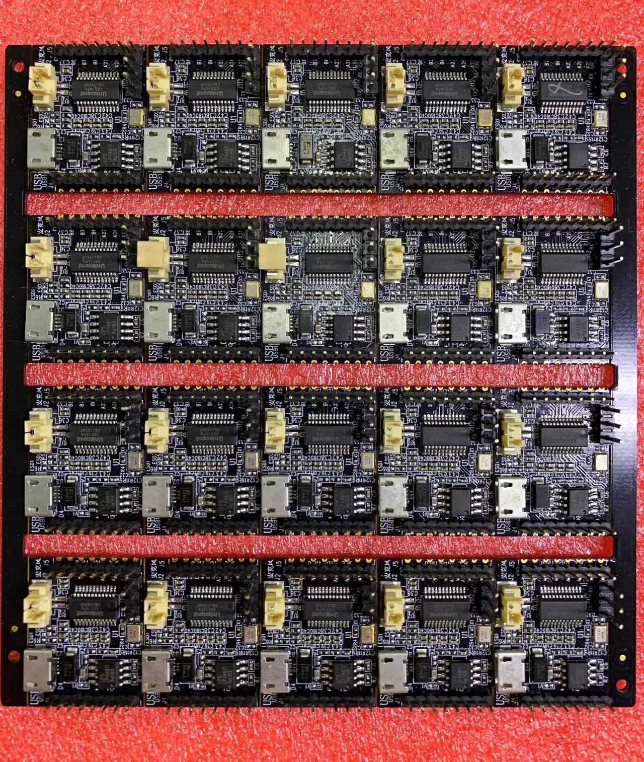
PCB Panel rules and methods
1. According to the process requirements of different assembly factories, the maximum size and minimum size of the panel should be clearly understood. Generally, PCB smaller than 80X80mm need to be panelized, and the maximum size depends on the processing capacity of the factory. In short, pcb size should meet the requirement of SMT equipment fittings, which is conducive to SMT patch processing and help to decide thickness of the PCB board.
2. The assembly and sub-boarding must meet the requirements of DFM and DFA, and at the same time ensure that the PCB assembly is fixed and not easily deformed after being placed on the fixture. The dividing groove between the panels should meet the flatness requirements of the surface during PCBA chip processing.
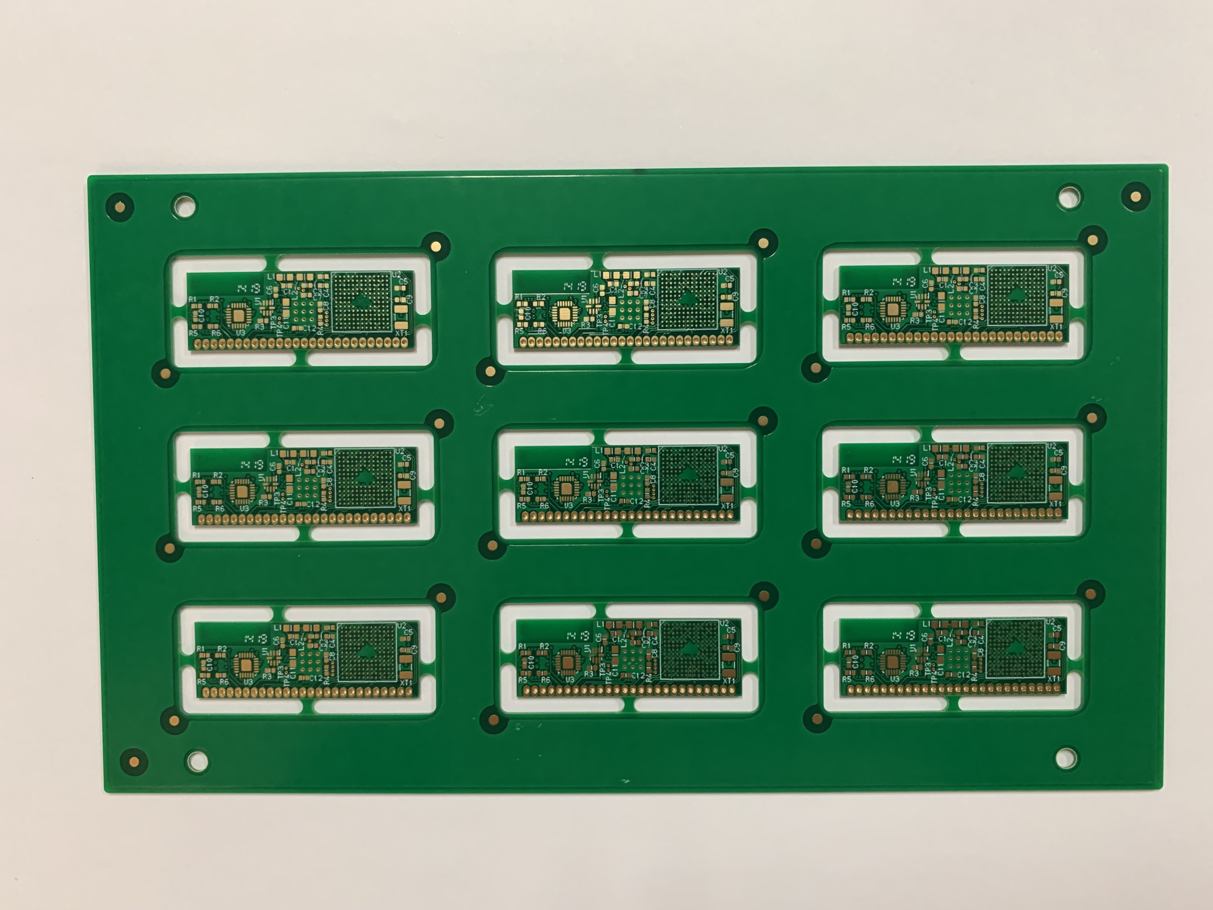
3. In PCB panel design, the arrangement of components should avoid splitting stress and cause component cracks. The use of pre-scored panel structure can minimize warpage and deformation during board separation, and reduce the stress on components. To a minimum, try not to place valuable components next to the process side.
4. The size and form of the panel are handled according to the specific project, and the appearance design is as close to the square as possible. It is strongly recommended to use the 2×2 or 3×3 panel method. It is not recommended to combine yin and yang panels if it is not necessary;
5. When the outline of the board edge connector exceeds the interference between the multi-joint boards, it is solved by rotating the joint + process side to prevent the poor quality of the collision damage during the transmission or handling process after welding.
6. After the panel design, it must be ensured that the edge of the reference point of the large board is at least 3.5mm away from the edge of the board (the minimum range of the machine clamping the edge of the PCB is 3.5mm), and the two diagonal reference points on the large board cannot be placed symmetrically. Do not place the reference points symmetrically, so that the reverse/reverse side of the PCB can enter the machine through the identification function of the device itself.
7. When the thickness of the PCB board is less than 1.0mm, the strength of the whole panel board will be greatly reduced (weakened) when the splicing joint or v-cut groove is added, because the V-cut depth is 1/3 of the board thickness , The middle of the PCB board is used for strength, and a part of the supporting skeleton - the glass fiber cloth V is broken, resulting in a significant softening of the strength. If it is not supported by a jig, it will affect the process below the PCBA.
8. When there are gold fingers on the PCB, generally place the gold fingers on the outside of the board in the direction of the non-splint position. The edge of the gold finger cannot be spliced or processed.
Shenzhen ANKE PCB Co.,LTD
Post time: Apr-04-2023


