


Electrical engineers often face the dilemma of determining the optimal number of layers for a PCB design. Is it better to use more layers or fewer layers? How do you make the decision on the number of layers for a PCB?
1.What does PCB layer mean?
The layers of a PCB refer to the copper layers that are laminated with the substrate. Except for single-layer PCBs that have only one copper layer, all PCBs with two or more layers have an even number of layers. The components are soldered onto the outermost layer, while the other layers serve as wiring connections. However, some high-end PCBs will also embed components within the inner layers.
PCBs are used to manufacture various electronic devices and machinery in different industries, such as consumer electronics, automotive, telecommunications, aerospace, military, and medical
industries. The number of layers and size of a specific board determines the power and capacity of the PCB. As the number of layers increases, so does the functionality.
2.How to Determine the Number of PCB Layers?
When deciding on the appropriate number of layers for a PCB, it is important to consider the benefits of using multiple layers versus single or double layers. At the same time, it is also necessary to consider the advantages of using a single layer design versus those of multilayer designs. These factors can be evaluated from the following five perspectives:
2-1. Where will the PCB be used?
When determining the specifications for a PCB board, it is crucial to consider the intended machine or equipment that the PCB will be used in, as well as the specific circuit board requirements for such equipment. This includes identifying whether the PCB board will be used in sophisticated and
complex electronic products, or in simpler products with basic functionality.
2-2. What working frequency is needed for the PCB?
The issue of working frequency needs to be considered when designing a PCB since this parameter determines the functionality and capacity of the PCB. For higher speed and operational capabilities, multi-layer PCBs are essential.
2-3.What is the project budget?
Other factors to consider are the manufacturing costs of single
and double layer PCBs versus multi-layer PCBs. If you want a PCB with as high a capacity as possible, the cost will inevitably be relatively high.
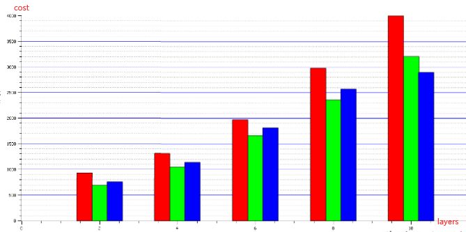
Some people ask about the relationship between the number of layers in a PCB and its price. Generally, the more layers a PCB has, the higher its price. This is because designing and manufacturing a multi-layer PCB takes longer and therefore costs more. The chart below shows the average cost of multi-layer PCBs for three different manufacturers under the following conditions:
PCB order quantity: 100;
PCB size: 400mm x 200mm;
Number of layers: 2, 4, 6, 8, 10.
The chart displays the average price of PCBs from three different companies, not including shipping costs. The cost of a PCB can be evaluated using PCB quotation websites, which allow you to select different parameters such as conductor type, size, quantity, and number of layers. This chart only provides a general idea of the average PCB prices from three manufacturers, and the prices may vary according to the number of layers. Shipping costs are not included. Effective calculators are available online, provided by manufacturers themselves to help customers evaluate the cost of their printed circuits based on different parameters such as conductor type, size, quantity, number of layers, insulation materials, thickness, etc.
2-4. What is the required delivery time for the PCB?
Delivery time refers to the time it takes to manufacture and deliver single/double/multilayer PCBs. When you need to produce a large quantity of PCBs, delivery time needs to be taken into account. The delivery time for single/double/multilayer PCBs varies and depends on the size of the PCB area. Of course, if you are willing to spend more money, the delivery time may be shortened.
2-5. What density and signal layer does the PCB require?
The number of layers in a PCB depends on the pin density and signal layers. For example, a pin density of 1.0 requires 2 signal layers, and as the pin density decreases, the number of layers required will increase. If the pin density is 0.2 or less, at least 10 layers of PCB are required.
3.Advantages of Different PCB Layers - Single-layer/Double-layer/Multi-layer.
3-1. Single-layer PCB
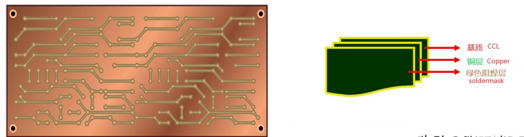
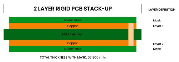
The construction of a single-layer PCB is simple, consisting of a single layer of pressed and welded layers of electrically conductive material. The first layer is covered with a copper-clad plate, and then a solder-resist layer is applied. The diagram of a single-layer PCB usually shows three colored strips to represent the layer and its two covering layers - gray for the dielectric layer itself, brown for the copper-clad plate, and green for the solder-resist layer.
Advantages:
● Low manufacturing cost, especially for the production of consumer electronics, which has a higher cost efficiency.
● Assembly of components, drilling, soldering, and installation are relatively simple, and the production process is less likely to encounter problems.
● Economical and suitable for mass production.
●Ideal choice for low-density designs.
Applications:
● Basic calculators use single-layer PCBs.
● Radios, such as low-priced radio alarm clocks in general merchandise stores, typically use single-layer PCBs.
● Coffee machines often use single-layer PCBs.
● Some household appliances use single-layer PCBs.
3-2. Double-layer PCB
Double-layer PCB has two layers of copper plating with an insulating layer in between. Components are placed on both sides of the board, which is why it is also called a double-sided PCB. They are manufactured by connecting two layers of copper together with a dielectric material in between, and each side of the copper can transmit different electrical signals. They are suitable for applications that require high speed and compact packaging.
Electrical signals are routed between the two layers of copper, and the dielectric material between them helps prevent these signals from interfering with each other. The double-layer PCB is the most common and economical circuit board to manufacture.
Double-layer PCBs are similar to single-layer PCBs, but have an inverted mirrored bottom half. When using double-layer PCBs, the dielectric layer is thicker than that of single-layer PCBs. Additionally, there is copper plating on both the top and bottom sides of the dielectric material. Furthermore, the top and bottom of the laminated board are covered with a solder resist layer.
The diagram of a double-layer PCB usually looks like a three-layer sandwich, with a thick gray layer in the middle representing the dielectric, brown stripes on the upper and lower layers representing the copper, and thin green stripes on the top and bottom representing the solder resist layer.
Advantages:
● Flexible design makes it suitable for a variety of devices.
● Low-cost structure which makes it convenient for mass production.
● Simple design.
● Small size suitable for various equipment.
Applications:
Double-layer PCBs are suitable for a wide range of simple and complex electronic devices. Examples of mass-produced equipment that feature double-layer PCBs include:
● HVAC units, residential heating and cooling systems from various brands all include double-layer printed circuit boards.
● Amplifiers, double-layer PCBs are equipped with amplifier units used by many musicians.
● Printers, various computer peripherals rely on double-layer PCBs.
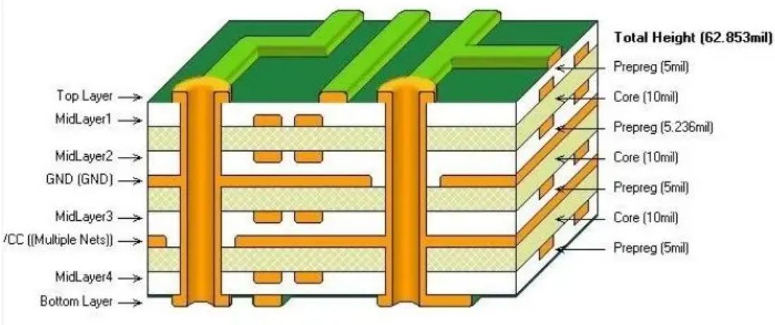
3-3. Four-layer PCB
A 4-layer PCB is a printed circuit board with four conductive layers: top, two inner layers, and bottom. Both inner layers are the core, typically used as a power or ground plane, while the outer top and bottom layers are used for placing components and routing signals.
The outer layers are usually covered with a solder resist layer with exposed pads to provide placement points for connecting surface-mounted devices and through-hole components. Through-holes are typically used to provide connections between the four layers, which are laminated together to form a board.
Here is the breakdown of these layers:
- Layer 1: Bottom layer, usually made of copper. It serves as the foundation of the entire circuit board, providing support for the other layers.
- Layer 2: Power layer. It's named this way because it provides clean and stable power to all components on the circuit board.
- Layer 3: Ground plane layer, serving as the ground source for all components on the circuit board.
- Layer 4: Top layer used for routing signals and providing connection points for components.
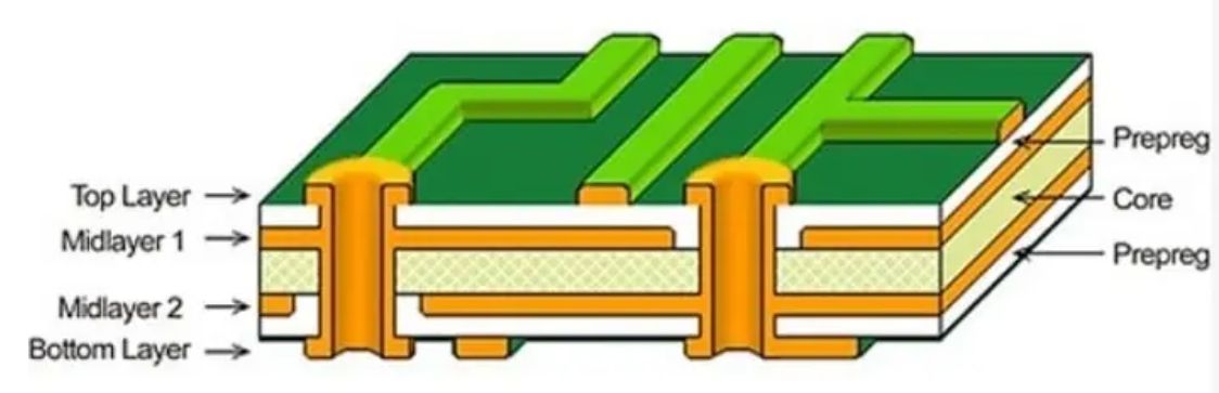
In a 4-layer PCB design, 4 copper traces are separated by 3 layers of internal dielectric and are sealed at the top and bottom with solder resist layers. Typically, the design rules for 4-layer PCBs are shown using 9 traces and 3 colors - brown for copper, gray for core and prepreg, and green for solder resist.
Advantages:
● Durability - Four-layer PCBs are more robust than single-layer and double-layer boards.
● Compact size - The small design of four-layer PCBs can fit a wide range of devices.
●Flexibility - Four-layer PCBs can work in multiple types of electronic devices, including simple and complex ones.
● Safety - By properly aligning the power and ground layers, four-layer PCBs can shield against electromagnetic interference.
● Lightweight - Devices equipped with four-layer PCBs require less internal wiring, so they are typically lighter in weight.
Applications:
● Satellite Systems - Multi-layer PCBs are equipped in orbiting satellites.
● Handheld Devices - Smartphones and tablets are typically equipped with four-layer PCBs.
● Space Exploration Equipment - Multi-layer printed circuit boards provide power to space exploration equipment.
3-4. 6 layers pcb
A 6-layer PCB is essentially a 4-layer board with two additional signal layers added between the planes. A standard 6-layer PCB stackup includes 4 routing layers (two outer and two inner) and 2 internal planes (one for ground and one for power).
Providing 2 internal layers for high-speed signals and 2 outer layers for low-speed signals significantly amplifies EMI (electromagnetic interference). EMI is the energy of signals within electronic devices being disrupted by radiation or induction.
There are various arrangements for the stackup of a 6-layer PCB, but the number of power, signal, and ground layers used depends on the application requirements.
A standard 6-layer PCB stackup includes top layer - prepreg - internal ground layer - core - internal routing layer - prepreg - internal routing layer - core - internal power layer - prepreg - bottom layer.
Although this is a standard configuration, it may not be suitable for all PCB designs, and it may be necessary to reposition the layers or have more specific layers. However, wiring efficiency and minimization of crosstalk must be considered when placing them.
Advantages:
● Strength - Six-layer PCBs are thicker than their thinner predecessors and therefore more robust.
● Compactness - Boards with six layers of this thickness have greater technical capabilities and can consume less width.
● High capacity - Six-layer or more PCBs provide optimal power for electronic devices and greatly reduce the possibility of crosstalk and electromagnetic interference.
Applications:
● Computers - 6-layer PCBs helped drive the rapid development of personal computers, making them more compact, lighter, and faster.
● Data storage - The high capacity of six-layer PCBs has made data storage devices increasingly abundant over the past decade.
● Fire alarm systems - Using 6 or more circuit boards, alarm systems become more accurate at the moment of detecting real danger.
As the number of layers in a printed circuit board increases beyond the fourth and sixth layer, more conductive copper layers and dielectric material layers are added to the stackup.
For example, an eight-layer PCB contains four planes and four signal copper layers - eight in total - connected by seven rows of dielectric material. The eight-layer stackup is sealed with dielectric solder mask layers on top and bottom. Essentially, the eight-layer PCB stackup is similar to the six-layer, but with an added pair of copper and prepreg column.
Shenzhen ANKE PCB Co.,LTD
2023-6-17
Post time: Jun-26-2023


