


Products
Industrial Main board PCBA projects manufacturing
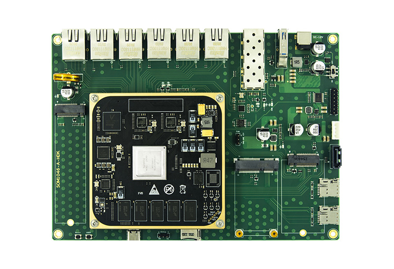
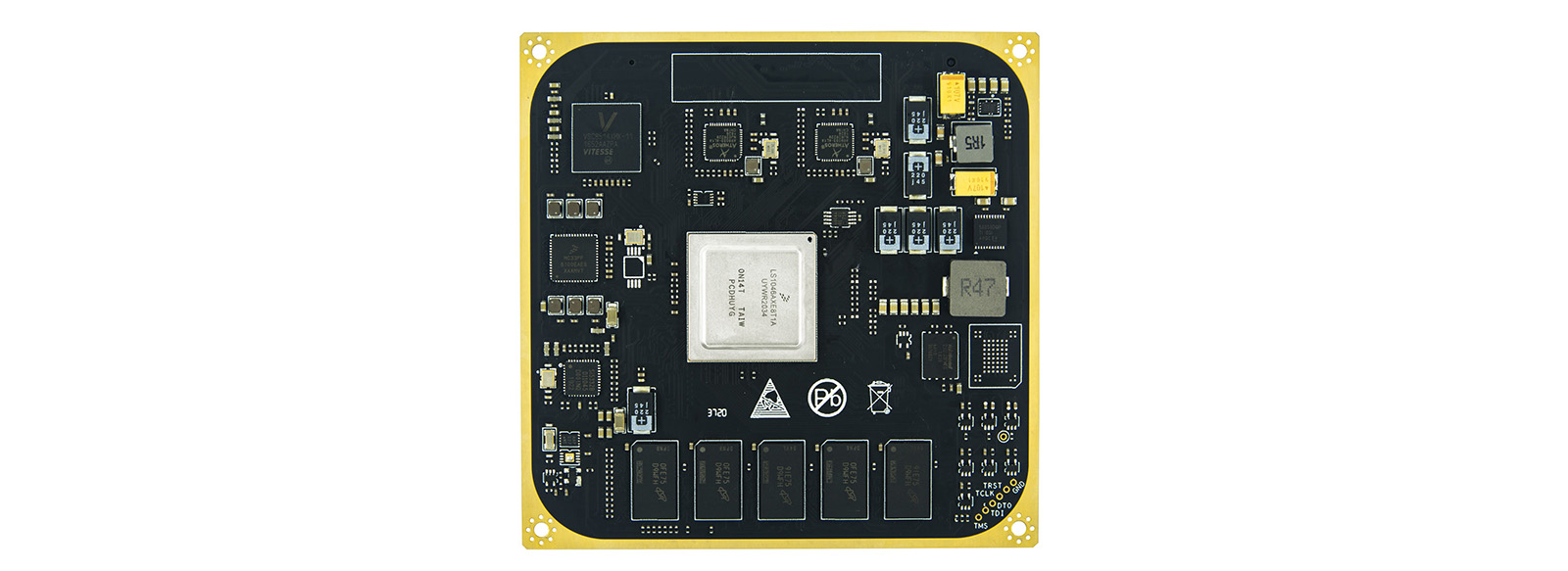
This is a PCB assembly project for Industrial Main board with IS1046. The industrial industry has been historically one of the major segment served by ANKE PCB yet we are now witnessing the Internet of Things, with a specific attention towards the Industrial Internet of Things (IOT), which will bring connectivity and automation to factories and companies around the world. As an automotive electronics company and automotive PCBA manufacturer, we, at ANKE, deliver high quality services in engineering, design and prototyping.
| Layers | 12 layers |
| Board thickness | 1.6MM |
| Material | Shengyi S1000-2 FR-4(TG≥170℃) |
| Copper thickness | 1oz(35um) |
| Surface Finish | ENIG Au Thickness 0.8um; Ni Thickness 3um |
| Min Hole(mm) | 0.13mm |
| Min Line Width(mm) | 0.15mm |
| Min Line Space(mm) | 0.15mm |
| Solder Mask | Green |
| Legend Color | White |
| Board size | 110*87mm |
| PCB assembly | Mixed surface mount assembly on both sides |
| ROHS complied | Lead FREE assembly process |
| Minimum components size | 0201 |
| Total components | 911 per board |
| IC packge | BGA,QFN |
| Main IC | Atmel, Micron, Maxim,Texas Instruments, On Semiconductor, Farichild,NXP |
| Test | AOI, X-ray, Functional Test |
| Application | Automotive electronics |
SMT Assembly Process
1. Place (curing)
Its role is to melt the patch glue so that the surface mount components and the PCB board are firmly bonded together.
The equipment used is a curing oven, located behind the placement machine in the SMT line.
2. Re-soldering
Its role is to melt the solder paste, so that the surface mount components and the PCB board are firmly bonded together. The equipment used was a reflow oven, located behind the pads.
Mounter on SMT production line.
3. SMT assembly cleaning
What it does is remove solder residues such as ux
The assembled PCB is harmful to human body. The equipment used is a washing machine, the location may be
Not fixed, it may be online or offline.
4. SMT assembly inspection
Its function is to check welding quality and assembly quality
The assembled PCB board.
The equipment used includes magnifying glass, microscope, in-circuit tester (ICT), needle tester, automatic optical inspection (AOI), X-RAY inspection system, functional tester, etc.
5. SMT assembly rework
Its role is to rework the failed PCB board
Fault. The tools used are soldering iron, rework station, etc.
anywhere on the production line. As you know, there are some small issues during production, so hand rework assembly is the best way.
6. SMT assembly packaging
PCBMay provides assembly, custom packaging, labeling, cleanroom production, sterilization management and other solutions to provide a complete custom solution for your company’s needs.
By using automation to assemble, package and validate our products, we can provide our
With more than 10 years experience as Electronic manufacturing service provider for Telecommunication, we ANKE support various devices and telecommunication protocols:
> Computing devices & equipment
> Servers & routers
> RF & Microwave
> Data centers
> Data storage
> Fiber optic devices
> Transceivers and transmitters

Electronic manufacturing service provider for Automotive, we cover numerous applications:
> Automotive camera product
> Temperature & humidity sensors
> Headlight
> Smart lighting
> Power modules
> Door controllers & door handles
> Body control modules
> Energy management
Layer Stackup
Stack-up refers to the arrangement of copper layers and insulating layers that make up a PCB prior to board layout design. While a layer stack-up allows you to get more circuitry on a single board through the various PCB board layers, the structure of PCB stackup design confers many other advantages:
• A PCB layer stack can help you minimize your circuit’s vulnerability to external noise as well as minimize radiation and reduce impedance and crosstalk concerns on high-speed PCB layouts.
• A good layer PCB stack-up can also help you balance your needs for low-cost, efficient manufacturing methods with concerns about signal integrity issues
• The right PCB layer stack can enhance the Electromagnetic Compatibility of your design as well.
It will very often be to your benefit to pursue a stacked PCB configuration for your printed circuit board-based applications.
For multilayer PCBs, general layers include ground plane (GND plane), power plane (PWR plane), and inner signal layers. Here’s a sample of an 8-layer PCB stackup.
ANKE PCB provides multilayer/high layers circuit boards in the range from 4 to 32 layers, board thickness from 0.2mm to 6.0mm, copper thickness from 18μm to 210μm (0.5oz to 6oz), inner layer copper thickness from 18μm to 70μm (0.5oz to 2oz), and minimal spacing between layers to 3mil.
Yes, we always use high quality export packaging. We also use specialized hazard packing for dangerous goods and validated cold storage shippers for temperature sensitive items. Specialist packaging and non-standard packing requirements may incur an additional charge.
The shipping cost depends on the way you choose to get the goods. Express is normally the most quickest but also most expensive way. By seafreight is the best solution for big amounts. Exactly freight rates we can only give you if we know the details of amount, weight and way. Please contact us for further information.


