


Products
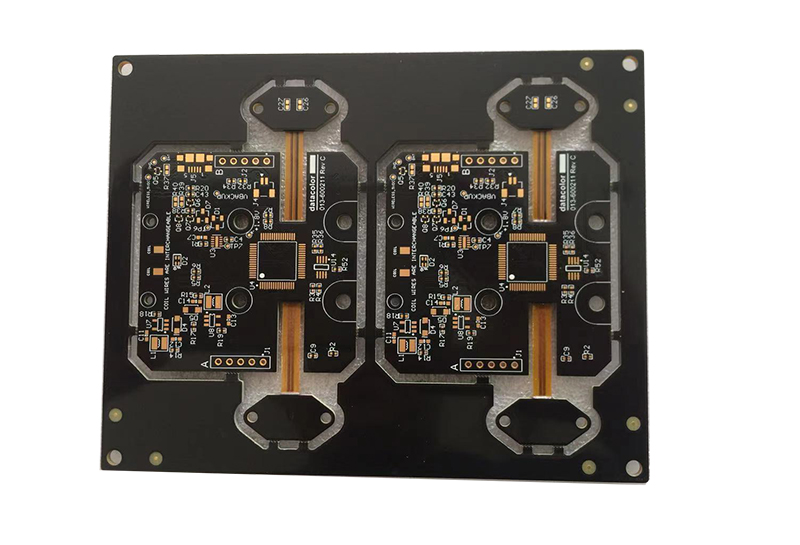
Industrial sensor 4 layer rigid&flex pcb with 2oz copper
| Layers | 4 layers rigid+2 layers flex |
| Board thickness | 1.60MM+0.2mm |
| Material | FR4 tg150+Polymide |
| Copper thickness | 1 OZ(35um) |
| Surface Finish | ENIG Au Thickness 1um; Ni Thickness 3um |
| Min Hole(mm) | 0.21mm |
| Min Line Width(mm) | 0.15mm |
| Min Line Space(mm) | 0.15mm |
| Solder Mask | Green |
| Legend Color | White |
| Mechanical processing | V-scoring, CNC Milling(routing) |
| Packing | Anti-static bag |
| E-test | Flying probe or Fixture |
| Acceptance standard | IPC-A-600H Class 2 |
| Application | Automotive electronics |
Introduction
Rigid&flex pcbs are combined with stiff boards to create this hybrid product. Some layers ofthe manufacturing process include a flexible circuit that runs through the rigid boards, resembling
a standard hardboard circuit design.
The board designer will add plated through holes (PTHs) that link stiff and flexible circuits as part of this process. This PCB was popular due to its intelligence, accuracy, and flexibility.
Rigid-Flex PCBs simplify the electronic design by removing flexible cables, connections, and individual wiring. A Rigid&Flex boards circuitry is more tightly integrated into the board’s overall structure, which improves electrical performance.
Engineers can expect significantly better maintainability and electrical performance thanks to the rigid-flex PCB’s internal electrical and mechanical connections.
Material
Substrate Materials
The most popular rigid-ex substance is woven fiberglass. A thick layer of epoxy resin coats this fiberglass.
Nevertheless, epoxy-impregnated fiberglass is uncertain. It can not withstand abrupt and sustained shocks.
Polyimide
This material is chosen for its flexibility. It is solid and can withstand shocks and motions.
Polyimide can also withstand heat. This makes it ideal for applications with temperature fluctuations.
Polyester (PET)
PET is favored for its electrical characteristics and flexibility. It resists chemicals and dampness. It may thus be employed in harsh industrial conditions.
Using a suitable substrate ensures desired strength and longevity. It considers elements like temperature resistance and dimension stability while selecting a substrate.
Polyimide Adhesives
The temperature elasticity of this adhesive makes it ideal for the job. It can withstand 500°C. Its high heat resistance makes it suitable for a variety of critical applications.
Polyester Adhesives
These adhesives are more cost saving than polyimide adhesives.
They are great for making basic rigid explosion proof circuits.
Their relationship is also weak. Polyester adhesives are also not heat resistant. They have been updated recently. This provides them with heat resistance. This change also promotes adaptation. This makes them safe in multilayer PCB assembly.
Acrylic Adhesives
These adhesives are superior. They have excellent thermal stability against corrosion and chemicals. They are easy to apply and relatively inexpensive. Combined with their availability, they are popular among manufacturers. manufacturers.
Epoxies
This is probably the most widely used adhesive in rigid-flex circuit manufacturing. They can also withstand corrosion and high and low temperatures.
They are also extremely adaptable and adhesively stable. It has a little polyester in it which makes it more flexible.
Stack-up
The stack-up of rigid-ex PCB is one of the most parts during
rigid-ex PCB fabrication and it’s more complicated than standard
rigid boards, let’s have a look at 4 layers of rigid-ex PCB as below:
Top solder mask
Top layer
Dielectric 1
Signal layer 1
Dielectric 3
Signal layer 2
Dielectric 2
Bottom layer
Bottom soldermask
PCB Capacity
| Rigid board capacity | |
| Number of layers: | 1-42 layers |
| Material: | FR4\high TG FR4\Lead free material\CEM1\CEM3\Aluminum\Metal core\PTFE\Rogers |
| Out layer Cu thickness: | 1-6OZ |
| Inner layer Cu thickness: | 1-4OZ |
| Maximum processing area: | 610*1100mm |
| Minimum board thickness: | 2 layers 0.3mm (12mil) 4 layers 0.4mm (16mil)6 layers 0.8mm (32mil)8 layers 1.0mm (40mil)
10 layers 1.1mm (44mil) 12 layers 1.3mm (52mil) 14 layers 1.5mm (59mil) 16 layers 1.6mm (63mil) |
| Minimum Width: | 0.076mm (3mil) |
| Minimum Space: | 0.076mm (3mil) |
| Minimum hole size (final hole): | 0.2mm |
| Aspect ratio: | 10:1 |
| Drilling hole size: | 0.2-0.65mm |
| Drilling tolerance: | +\-0.05mm(2mil) |
| PTH tolerance: | Φ0.2-1.6mm +\-0.075mm (3mil) Φ1.6-6.3mm+\-0.1mm(4mil) |
| NPTH tolerance: | Φ0.2-1.6mm +\-0.05mm(2mil) Φ1.6-6.3mm+\-0.05mm(2mil) |
| Finish board tolerance: | Thickness<0.8mm, Tolerance:+/-0.08mm |
| 0.8mm≤Thickness≤6.5mm,Tolerance+/-10% | |
| Minimum soldermask bridge: | 0.076mm (3mil) |
| Twisting and bending: | ≤0.75% Min0.5% |
| Raneg of TG: | 130-215℃ |
| Impedance tolerance: | +/-10%,Min+/-5% |
| Surface Treatment: | HASL, LF HASL |
| Immersion Gold, Flash Gold,Gold finger | |
| Immersion Silver, Immersion Tin,OSP | |
| Selective Gold Plating, Gold thickness up to 3um(120u”) | |
| Carbon Print, Peelable S/M,ENEPIG | |
| Aluminum board capacity | |
| Number of layers: | Single layer, double layers |
| Maximum board size: | 1500*600mm |
| Board thickness: | 0.5-3.0mm |
| Copper thickness: | 0.5-4oz |
| Minimum hole size: | 0.8mm |
| Minimum width: | 0.1mm |
| Minimum space: | 0.12mm |
| Minimum pad size: | 10 micron |
| Surface finish: | HASL,OSP,ENIG |
| Shaping: | CNC, Punching, V-cut |
| Equipement: | Universal Tester |
| Flying Probe Open/Short Tester | |
| High power Microscope | |
| Solderability Testing Kit | |
| Peel Strength tester | |
| High Volt Open & Short tester | |
| Cross Section Molding Kit With Polisher | |
| FPC Capacity | |
| Layers: | 1-8 layers |
| Board thickness: | 0.05-0.5mm |
| Copper thickness: | 0.5-3OZ |
| Minimum Width: | 0.075mm |
| Minimum space: | 0.075mm |
| In through hole size: | 0.2mm |
| Minimum laser hole size: | 0.075mm |
| Minimum punching hole size: | 0.5mm |
| Soldermask tolerance: | +\-0.5mm |
| Minimum routing dimension tolerance: | +\-0.5mm |
| Surface finish: | HASL,LF HASL, Immersion Silver, Immersion Gold,Flash Gold, OSP |
| Shaping: | Punching, Laser, Cut |
| Equipement: | Universal Tester |
| Flying Probe Open/Short Tester | |
| High power Microscope | |
| Solderability Testing Kit | |
| Peel Strength tester | |
| High Volt Open & Short tester | |
| Cross Section Molding Kit With Polisher | |
|
Rigid&flex capacity |
|
| Layers: | 1-28 layers |
| Material type: | FR-4(High Tg, Halogen Free, High Frequency) PTFE, BT, Getek, Aluminium base,Copper base,KB, Nanya, Shengyi, ITEQ, ILM, Isola, Nelco, Rogers, Arlon |
| Board thickness: | 6-240mil/0.15-6.0mm |
| Copper thickness: | 210um (6oz) for inner layer 210um (6oz) for outer layer |
| Min mechanical drill size: | 0.2mm/0.08” |
| Aspect ratio: | 2:1 |
| Max panel size: | Sigle side or double sides:500mm*1200mm |
| Multilayer layers:508mm X 610mm (20″ X 24″) | |
| Min line width/space: | 0.076mm / 0.076mm (0.003″ / 0.003″)/ 3mil/3mil |
| Via hole type: | Blind / Buried / Plugged(VOP,VIP…) |
| HDI / Microvia: | YES |
| Surface finish: | HASL, LF HASL |
| Immersion Gold, Flash Gold,Gold finger | |
| Immersion Silver, Immersion Tin,OSP | |
| Selective Gold Plating, Gold thickness up to 3um(120u”) | |
| Carbon Print, Peelable S/M,ENEPIG | |
| Shaping: | CNC, Punching, V-cut |
| Equipement: | Universal Tester |
| Flying Probe Open/Short Tester | |
| High power Microscope | |
| Solderability Testing Kit | |
| Peel Strength tester | |
| High Volt Open & Short tester | |
| Cross Section Molding Kit With Polisher | |


