


Products
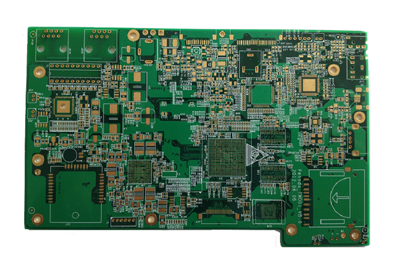
10 layer HDI for Military & Defence market of IPC 3 standard
| Layers | 10 layers |
| Board thickness | 2.4MM |
| Material | FR4 tg170 |
| Copper thickness | 1/1/1/1/1/1/1/1/1/1 OZ(35um) |
| Surface Finish | ENIG Au Thickness 0.05um; Ni Thickness 3um |
| Min Hole(mm) | 0.203mm filled with resin |
| Min Line Width(mm) | 0.1mm/4mil |
| Min Line Space(mm) | 0.1mm/4mil |
| Solder Mask | Green |
| Legend Color | White |
| Mechanical processing | V-scoring, CNC Milling(routing) |
| Packing | Anti-static bag |
| E-test | Flying probe or Fixture |
| Acceptance standard | IPC-A-600H Class 2 |
| Application | Automotive electronics |
Introduction
HDI is an abbreviation for High-Density Interconnect. It is a complex PCB design technique. HDI PCB technology can shrink printed circuit boards in the PCB field. The technology also provides high performance and greater density of wires and circuits.
By the way, HDI circuit boards are designed differently than normal printed circuit boards.
HDI PCBs are powered by smaller vias, lines and spaces. HDI PCBs are very lightweight, which is closely related to their miniaturization.
On the other hand, HDI is characterized by high frequency transmission, controlled redundant radiation, and controlled impedance on the PCB. Due to the miniaturization of the board, the board density is high.
Microvias, blind and buried vias, high performance, thin materials and fine lines are all hallmarks of HDI printed circuit boards.
Engineers must have a thorough understanding of the design and HDI PCB manufacturing process. Microchips on HDI printed circuit boards require special attention throughout the assembly process, as well as excellent soldering skills.
In compact designs like laptops, mobile phones, HDI PCBs are smaller in size and weight. Due to their smaller size, HDI PCBs are also less prone to cracks.
HDI Vias
Vias are holes in a PCB that are used to electrically connect different layers in the PCB. Using multiple layers and connecting them with vias reduces PCB size. Since the main goal of an HDI board is to reduce its size, vias are one of its most important factors. There are different types of through holes.

Through hole via
It goes through the entire PCB, from the surface layer to the bottom layer, and is called a via. At this point, they connect all layers of the printed circuit board. However, vias take up more space and reduce component space.
Blind via
Blind vias simply connect the outer layer to the inner layer of the PCB. No need to drill the entire PCB.
Buried via
Buried vias are used to connect the inner layers of the PCB. Buried vias are not visible from the outside of the PCB.
Micro via
Micro vias are the smallest via size less than 6 mils. You need to use laser drilling to form micro vias. So basically, microvias are used for HDI boards. This is because of its size. Since you need component density and cannot waste space in an HDI PCB, it is wise to replace other common vias with microvias. Additionally, microvias do not suffer from thermal expansion issues (CTE) because of their shorter barrels.
Stackup
HDI PCB stack-up is a layer-by-layer organization. The number of layers or stacks can be determined as required. However, this could be 8 layers to 40 layers or more.
But the exact number of layers depends on the density of the traces. Multilayer stacking can help you reduce PCB size. It also reduces manufacturing costs.
By the way, to determine the number of layers on an HDI PCB, you need to determine the trace size and the nets on each layer. After identifying them, you can calculate the layer stackup required for your HDI board.
Tips to design HDI PCB
1. Precise component selection. HDI boards require high pin count SMDs and BGAs smaller than 0.65mm. You need to choose them wisely as they affect via type, trace width and HDI PCB stack-up.
2. You need to use microvias on the HDI board. This will allow you to get double the space of a via or other.
3. Materials that are both effective and efficient must be used. It is critical to the manufacturability of the product.
4. To get a flat PCB surface, you should fill the via holes.
5. Try to choose materials with the same CTE rate for all layers.
6. Pay close attention to thermal management. Make sure you properly design and organize the layers that can properly dissipate excess heat.
About:
Located in Shenzhen, ANKE PCB is a professional PCB production service provider with more than 10 years of experience in the electronics manufacturing industry. We’ve manufactured printed circuit boards and assembly service over 80 countries around the world. Our customer satisfaction rate is around 99%, and we take pride in providing the best service around.
We specialize in providing companies with full-range and high-quality PCB fabrication, PCB assembly and components sourcing services of prototype, small/medium/high volume products on the basis of 2,000 square meters and skilled employees over 400. We are dedicated to providing a complete electronic service that will help PCB designers bring their projects to market on time and on budget.
Our prices are subject to change depending on supply and other market factors. We will send you an updated price list after your company contact us for further information.
The shipping cost depends on the way you choose to get the goods. Express is normally the most quickest but also most expensive way. By seafreight is the best solution for big amounts. Exactly freight rates we can only give you if we know the details of amount, weight and way. Please contact us for further information.
Yes, we always use high quality export packaging. We also use specialized hazard packing for dangerous goods and validated cold storage shippers for temperature sensitive items. Specialist packaging and non-standard packing requirements may incur an additional charge.
For samples, the lead time is about 7 days. For mass production, the lead time is 20-30 days after receiving the deposit payment. The lead times become effective when (1) we have received your deposit, and (2) we have your final approval for your products. If our lead times do not work with your deadline, please go over your requirements with your sale. In all cases we will try to accommodate your needs. In most cases we are able to do so.
Yes, we can provide most documentation including Certificates of Analysis / Conformance; Insurance; Origin, and other export documents where required.


